Pcb altium layout supply power embedded engineering system 3v layer example double just Altium schematic connection follow order make wires pcb How to create a pcb schematic
Embedded System Engineering: Altium Designer Tutorial 4 - PCB Layout
Altium designer crack key latest license panel build requirements essential system which Altium pcb Pcb design
Altium pcb layout
Altium componentAltium how to make it to follow net connection order.. Learn altium essentialsHow to create a pcb schematic.
Embedded system engineering: altium designer tutorial 4Gnd altium pour pad connect pcb specific make Altium designer 20.1.10 build 176 crack full license key [latest]4 layers pcb designing in altium : schematic design tutorial.

Altium schematic pcb
.
.


Altium how to make it to follow net connection order.. - Page 1

4 Layers PCB Designing in Altium : Schematic Design tutorial - YouTube
![Altium Designer 20.1.10 Build 176 Crack Full License Key [Latest]](https://i2.wp.com/warezcrack.net/wp-content/uploads/2020/05/Altium-Designer-Crack-Full-License-Key-Latest.jpg)
Altium Designer 20.1.10 Build 176 Crack Full License Key [Latest]
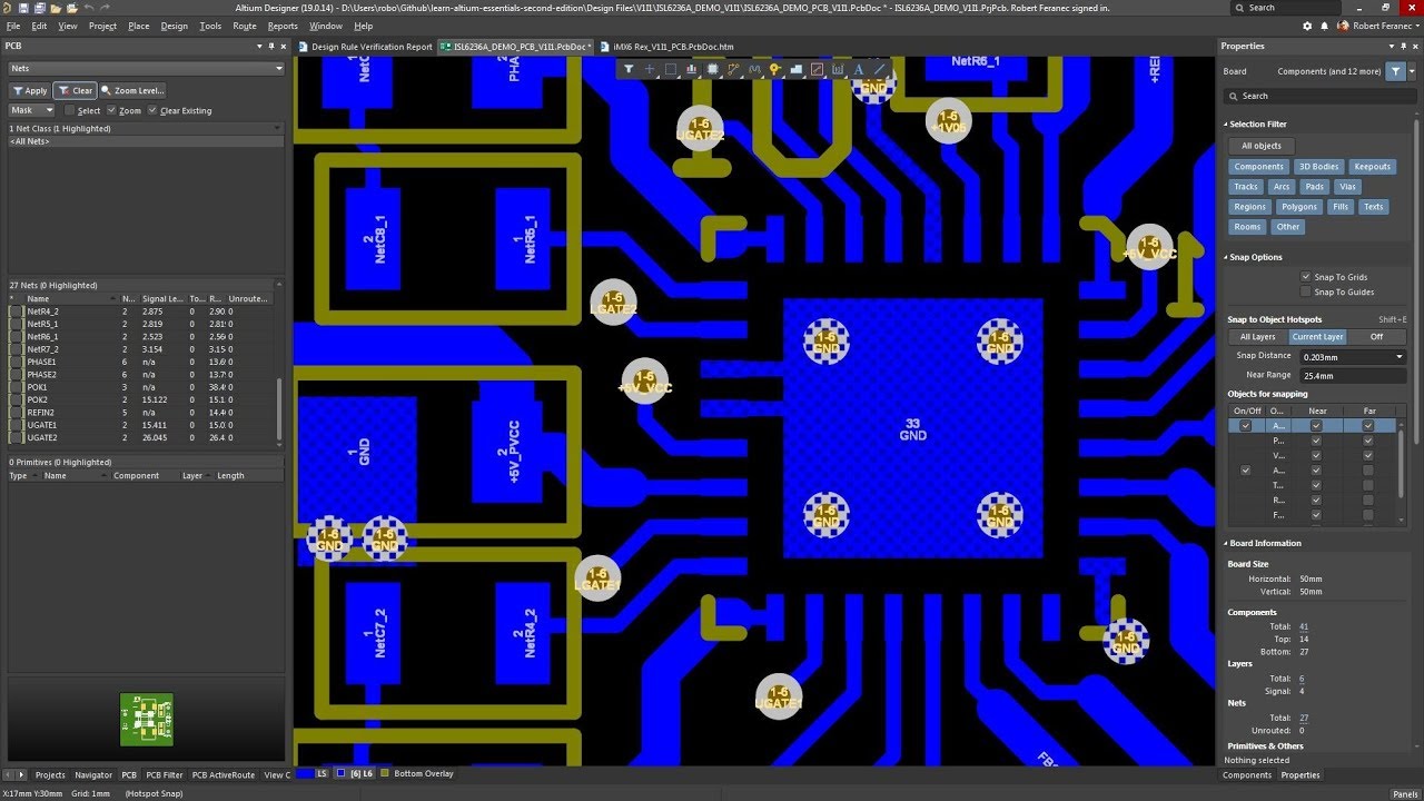
Learn Altium Essentials - Doing PCB Layout (Lesson 4) - Second Edition

pcb design - Altium: make a specific GND pad not to connect to GND pour

Embedded System Engineering: Altium Designer Tutorial 4 - PCB Layout
