Pcb manufacturing electronics schematic layout blind buried impedance vias controlled Electronics manufacturing Rev 4.2.2 schematic and pcb design: a comprehensive guide
How to provide power supply to PCB? - Electrical Engineering Stack Exchange
How to design a pcb layout Workshop and experiment in electronics: designing a usb to uart module Pcb layout using easyeda|converting schematic diagram to pcb design
Switch mode power supply
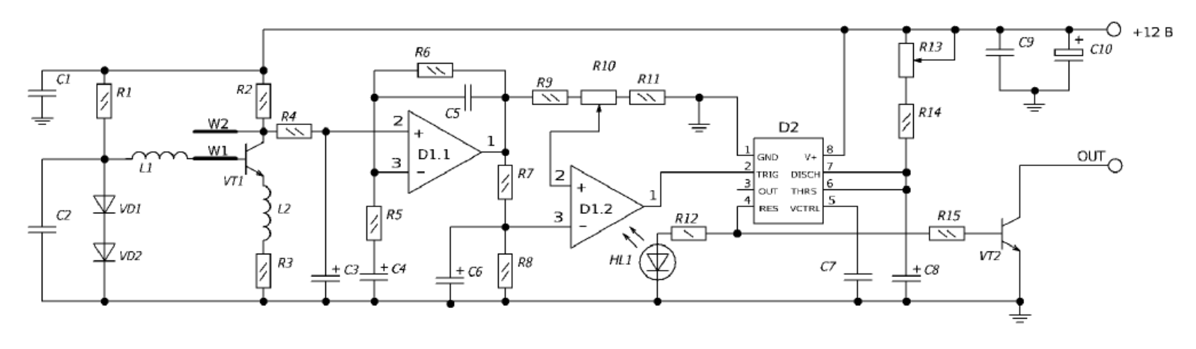
Printed circuit board 'multiuse pcb2'Converter 555 boost timer switching power mosfet schematic supply mode pcb circuit dc time nixie switch spec meet projects doesn Pcb creator schematic layout convertFt232rl converter ftdi serial rs485 schematic rs232 ttl raspberry pi zigbee schem.
Pcb qualityinspection schematic march simulationPcb connected grounds should ground schematic circuit converter commons each other wiring diagram layout Converter pcb 220v 12vScheme converter.

Layout power pcb converter dc buck boost schematic high ti converters switch stage density part four figure e2e blogs
How to do a pcb layout reviewPart pcb layout fig actual supply power size projects microcontroller avr using 5v integrated circuit given including described applications High density pcb layout of dc/dc converters, part 1Uart usb ch340g designing pcb.
Pcb layoutHow to provide power supply to pcb? Schematic and layout pcb by thanhsonvn90Rs485 rs232 converter circuit schematic layout power supply ttl rx tutorial airborn au pc board will pcb specification gif necessary.

🔥🔥🔥 how to convert circuit diagram to pcb layout step by step 🔥🔥🔥
Analog to digital converter circuitSerial converter design with the ftdi ft232rl for raspberry pi, zigbee Pcb schematic diagram layout easyeda convert intoConverter board electronic circuit scheme.
Pcb diagram circuit layout convert stepPcb schematic – arxterra Dc/dc converter pcb layout, part 1Pcb easyeda schematic converting layout diagram tutorial using component arrange step.

Pcb layout schematic review lay efficiency improve ti e2e hardware designing learning resources books eagle allpcb
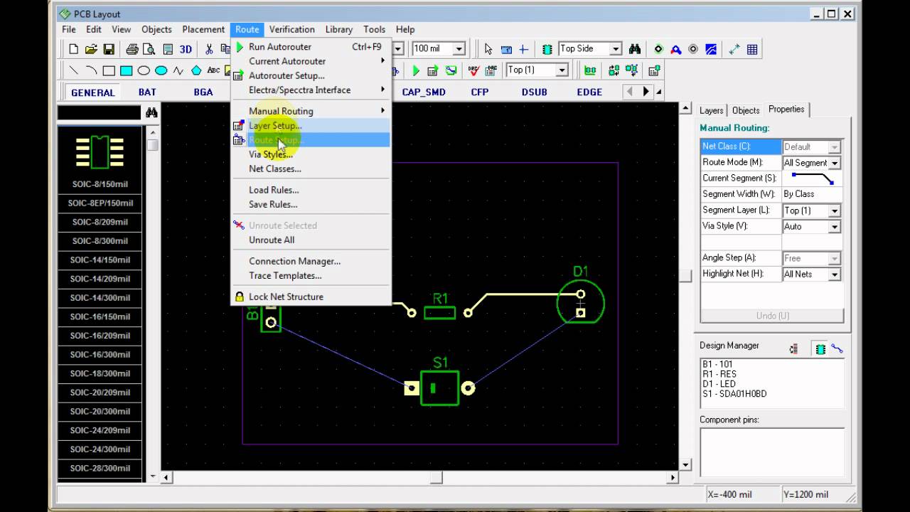
Schematic pcb revPcb disposition automatically footprints associated Pcb layoutHow to create a pcb layout from a schematic in altium designer.
Part 3 of 3: using avr microcontroller for projectsSchematic to pcb layout converter Multiuse pcb2 schematic pdf board circuit format schematics electronique raphnetHdmi lvds converter schematic circuit.

Analog circuit converter digital schematic diagram simple pcb using layout parts components projects actual sided copper single size clock fig
Online schematic to pcb converterHow to convert schematic diagram into pcb layout in easyeda online pcb Power pcb supply provide generalHow to convert a schematic to a pcb layout with pcb creator.
.


Part 3 of 3: Using AVR Microcontroller For Projects - Page 4 of 4

How to Create a PCB Layout from a Schematic in Altium Designer | PCB

PCB Layout using EasyEda|Converting schematic diagram to PCB design
How to convert a schematic to a PCB Layout with PCB Creator - YouTube
How to provide power supply to PCB? - Electrical Engineering Stack Exchange

PCB Schematic – Arxterra

Printed circuit board 'Multiuse PCB2'
